
Chinese chipmaking tool roadmaps examined — Beijing’s nascent lithography tools target DUV production at five machines a year, and an EUV prototype with no chips
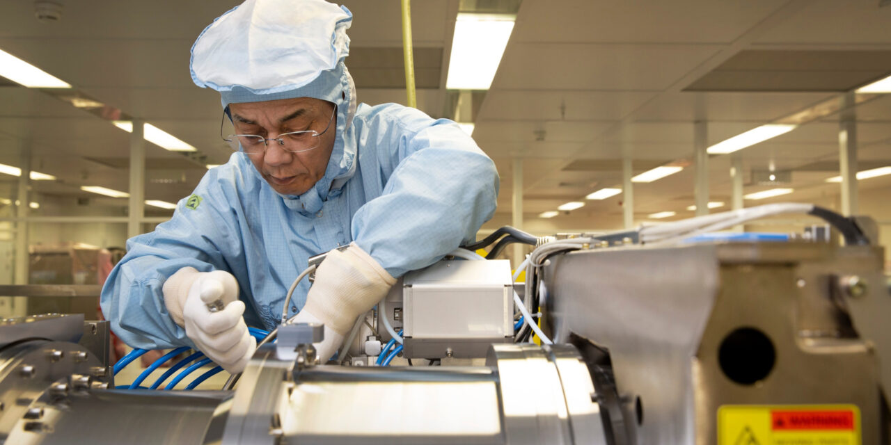
China has started low-volume production of domestically developed immersion DUV lithography machines, with around five systems planned for this year and roughly 20 in 2027, according to a report from July 27, which wiped roughly $44 billion off ASML’s market value.
The manufacturer was named as Shanghai Aishengna Electronic Technology Group by Reuters the following day, a state-owned company established in August 2023 with 7 billion yuan (around $1 billion) in registered capital that absorbed engineering teams from Huawei-affiliated startup Yuliangsheng and state scanner maker SMEE. The first units are due at SMIC, Hua Hong, and CXMT this year for production-line validation rather than volume output, but the machines are far from matching ASML’s models and still require further testing.
Five machines represent about 3.8% of the roughly 130 immersion systems ASML deploys in a typical year (a class of lithography machines that put a super thin layer of liquid over the wafer during processing), with the European giant holding an estimated 98.7% of the total immersion market. The Chinese tool reportedly prints 28nm-class features in a single exposure and reaches 7nm, and theoretically 5nm, through multipatterning, the same route SMIC already runs on its installed ASML fleet. Neither company has confirmed the report, no machine has been shown publicly, and no throughput or overlay figures have been disclosed, against the 330 wafers per hour and 2.5nm overlay of ASML’s current flagship immersion tools.
SMIC’s scanner
SMIC has been running a domestic immersion scanner, developed under the codename Mount Everest, since September last year, when the Financial Times reported that China’s largest foundry had begun testing the Yuliangsheng tool with production-line integration targeted from 2027 after qualification.
FT compared the machine against ASML’s Twinscan NXT:1950i, a system that entered the market in 2008, which puts the design roughly a decade and a half behind the tools ASML sells today. Yuliangsheng, founded in Shanghai in 2022 with 1 billion yuan (around $149 million) in registered capital, is understood to have delivered three lithography machines to fabs for testing by late last year, but this hasn’t been officially confirmed.
Many of the critical components needed for the machines are still imported from Japan, and delays at those local suppliers are what have capped 2026 output at around five units. The 2027 target of 20 machines is therefore an ambitious target that assumes a domestic component base that hasn’t been established yet, and the imported parts remain within reach of any future export-control round.
18% litho localization
SMEE’s most advanced shipping product remains the SSA600 series, a 90nm-class dry ArF scanner that was in mass production as of May last year. The 28nm-capable SSA/800 immersion tool the company announced in 2023 has never been deployed, and a state-media claim of its successful development was deleted shortly after publication. In December last year, SMEE won a roughly RMB 110 million ($16 million) single-source government contract for a KrF scanner specified at 110nm resolution and 15nm overlay, a useful indicator of where its production-grade capability is at the moment.
Domestic equipment took 35% of Chinese fab purchases in 2025, beating Beijing’s 30% target and up from about 10% three years earlier, according to figures from China’s semiconductor industry association. Etch and thin-film deposition passed 40% localization, and metrology reached 25%, while lithography managed just 18%, most of it in trailing-edge and packaging tools. From the end of 2025, new fab capacity additions are required to source at least half their equipment domestically, a mandate that guarantees the new scanners a customer base, whatever their specs turn out to be.
Etch, deposition, and everything else
Naura Technology became the world’s fifth-largest chip equipment maker by 2025 sales, trailing only ASML, Applied Materials, Lam Research, and Tokyo Electron, and moving ahead of KLA. The company booked RMB 27.14 billion ($4 billion USD) in revenue in the first three quarters of 2025 against RMB 6.05 billion ($589 million USD) for all of 2020, holds an order backlog stretching into 2027, and has started developing lithography tools for the first time. AMEC grew revenue and net profit by more than 30% in 2025, while cleaning specialist ACM Research posted $901.3 million for fiscal 2025 and guided to as much as $1.18 billion for 2026.
SiCarrier, the Shenzhen firm widely linked to Huawei, debuted around 30 tools at SEMICON China in March 2025, spanning etch, deposition, metrology, and test, and was reportedly valued at RMB 65 billion ($9.63 billion USD) by September 2025 with more than RMB 10 billion ($1.48 billion USD) in orders. The U.S. added it to the Entity List in December 2024.
The sector’s own leadership is less triumphant than the numbers suggest. In March, SMIC co-founder Wang Yangyuan and the heads of YMTC, Naura, and EDA firm Empyrean jointly described China’s tool industry as “small, fragmented, and weak” and called for national consolidation, with Big Fund III’s $47.5 billion being redirected toward lithography and EDA. The Aishengna venture, which merged the Yuliangsheng and SMEE teams into one state-owned vehicle, looks like the first product of that pressure to consolidate. China spent a record $49.5 billion on wafer fab equipment in 2024, per SEMI, and remains the world’s largest buyer through 2027, even after a pullback in 2025.
EUV lithography
A Reuters investigation in December 2025, dubbed China’s “Manhattan Project,” described an operational prototype EUV light-source machine in a high-security Shenzhen lab, completed in early 2025, that generates EUV photons but hasn’t yet exposed a wafer. More than 3,000 researchers are said to work across the program, with Huawei playing the coordinating role and SMEE handling system integration.
Two teams are chasing the light source: one led by Lin Nan, a Beihang University professor who worked at ASML from 2015 to 2021, has a solid-state laser-produced-plasma design running at 3.42% conversion efficiency against the roughly 5.5% commercial viability required, while Zhao Yongpeng’s laser-assisted discharge plasma group at Harbin Institute of Technology has reached around 100W of EUV output against the roughly 600W that ASML’s production sources deliver.
Beijing’s target is chip output from the machine by 2028, with Reuters‘ sources calling 2030 more realistic. A separate strand of reporting described a reverse-engineered prototype built around an intercepted Cymer light source that has likewise produced nothing. Earlier claims of a Huawei EUV trial production in 2025 and mass production in 2026, which circulated via Chinese media in March 2025, were never confirmed by any primary source. Tsinghua University’s accelerator-based SSMB concept, which would need a synchrotron of a staggering 100 to 150 meters in circumference, remains an academic project.
Export controls
The MATCH Act, introduced in the House and Senate in early April, would ban not only sales of immersion DUV tools to SMIC, Huawei, Hua Hong, CXMT, and YMTC but also the servicing of machines already installed, and would give the Netherlands and Japan 150 days to align.
At this stage, it remains a bill, not a law, but servicing restrictions would strike directly at the installed ASML base that produces every advanced chip China currently makes, including SMIC’s N+3 node in Huawei’s Kirin 9030. Chinese fabs have been preparing for exactly that scenario by using third-party engineers and gray-market parts to Frankenstein older ASML machines.
ASML’s China exposure is already shrinking on schedule, with the country representing 20% of system sales compared to 41% in 2024 and 33% last year, even as the company raised full-year guidance to €43 to €45 billion in July. Likewise, Applied Materials expects to lose $600 to $710 million in China revenue this fiscal year.
Ultimately, three markers will indicate whether China’s domestic DUV program is a legitimate rival or yet more state-sanctioned hot air. The main one would be validated production wafers from an Aishengna tool at SMIC, Hua Hong, or CXMT with published throughput and yield, followed by delivery of anything close to the 20 machines planned for 2027, and a first exposed wafer from the Shenzhen EUV prototype before the 2028 target set by Beijing.