Hot Chips 2026: Intel details cutting-edge tech in entry-level Wildcat Lake — value-focused 18A chips necessitated UCIe integration
This Tom’s Hardware Premium article is free to read with a Tom’s Hardware account; no payment necessary. We’re offering free access from August 23 to 26 so you can read all of our reporting from Hot Chips.
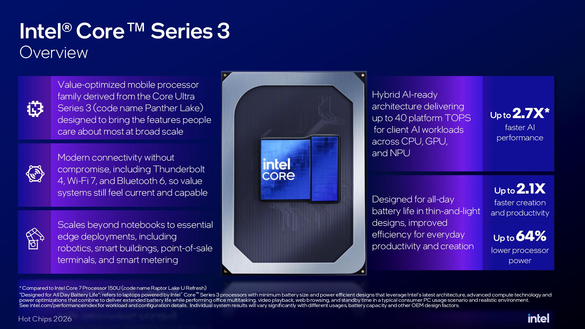
Intel’s Wildcat Lake is unassuming, launching with the message that it was a cutting-edge alternative to the MacBook Neo with Intel’s latest node and some trimmings around the edges. Although Wildcat Lake is, indeed, a budget part with major concessions to reach a market increasingly pushed to the side by powerful PC hardware, it also comes with a major innovation: UCIe.
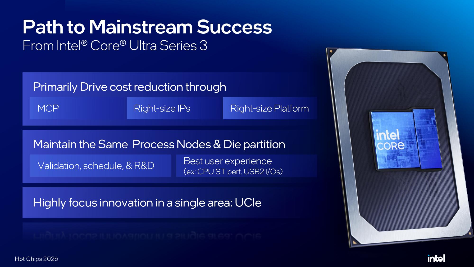
The Universal Chiplet Interconnect Express (UCIe) specification first debuted in 2022, coincidentally around the time that planning around Wildcat Lake began. Both AMD and Intel have rallied behind UCIe as an open interconnect communications standard, though they’ve primarily relied on their own chiplet communication technology like AMD’s Infinity Fabric. In Wildcat Lake, Intel leveraged UCIe to reduce cost. Further, it was a key technology that allowed Wildcat Lake to exist in the first place.
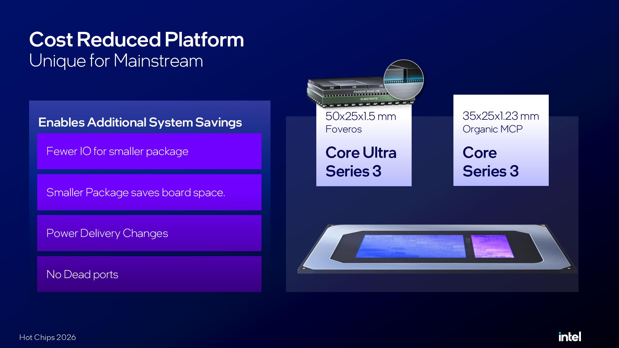
Opening the Hot Chips 2026 presentation, Intel’s Lance Hacking, lead engineer on Wildcat Lake, said the company had the choice between a monolithic design or a basic, low-cost Multi-Chip Package (MCP). Intel has Foveros for advanced 2.5D and 3D packaging, but for a budget part like Wildcat Lake, that wasn’t an option.
Choosing to leverage UCIe over an MCP design shaped the Wildcat Lake we have today, setting a roadmap for where Intel could cut compute to save cost and in areas where it would need to optimize to fit the necessary communication channels for the two chiplets.
UCIe integration in Intel Wildcat Lake
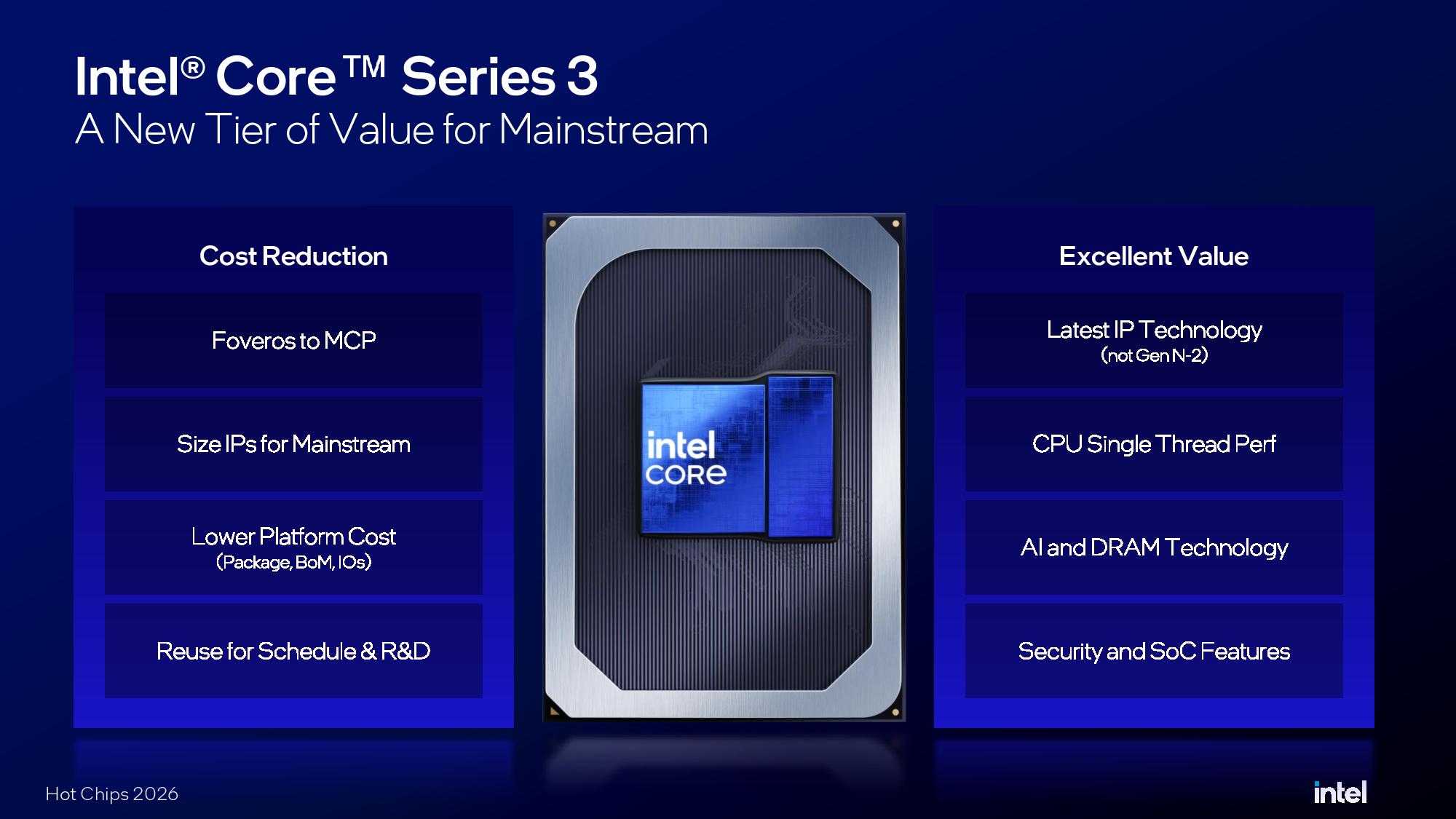
As Hacking explained during his presentation, budget parts usually involve an N-1 design. You leverage older IP, trim around the edges to improve the economics of yields, and repackage it as a mainstream part. Wildcat Lake is different in that regard. It’s taking Intel’s latest, most advanced, and most expensive IP for compute and applying it to the budget domain.
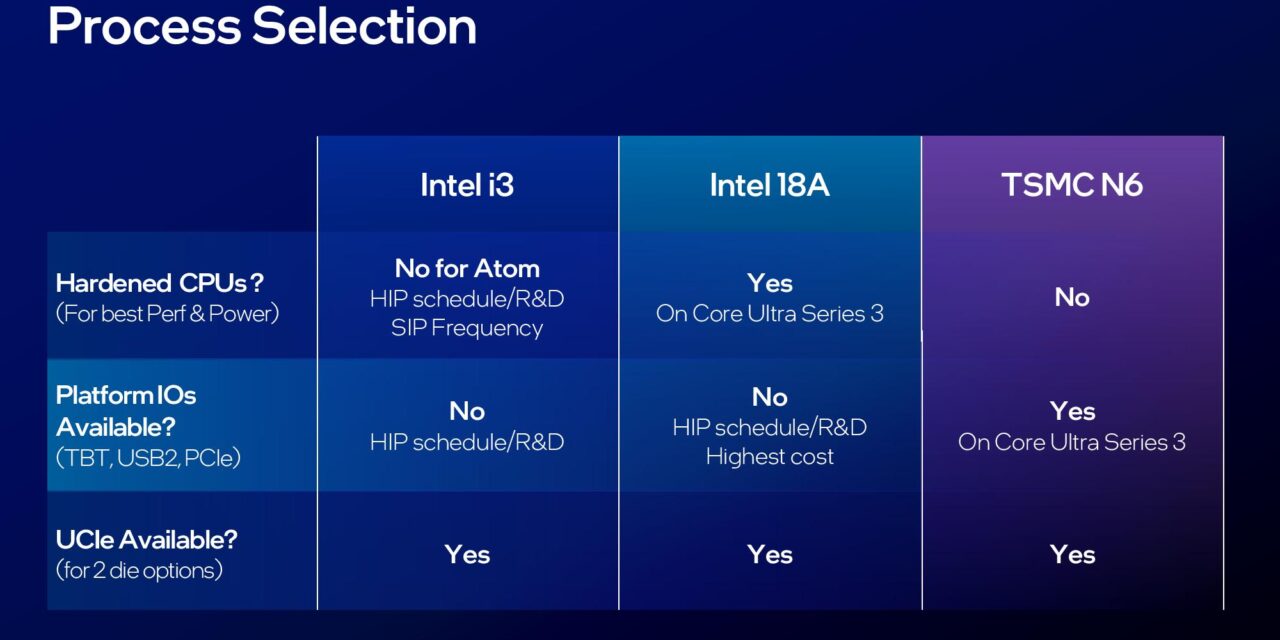
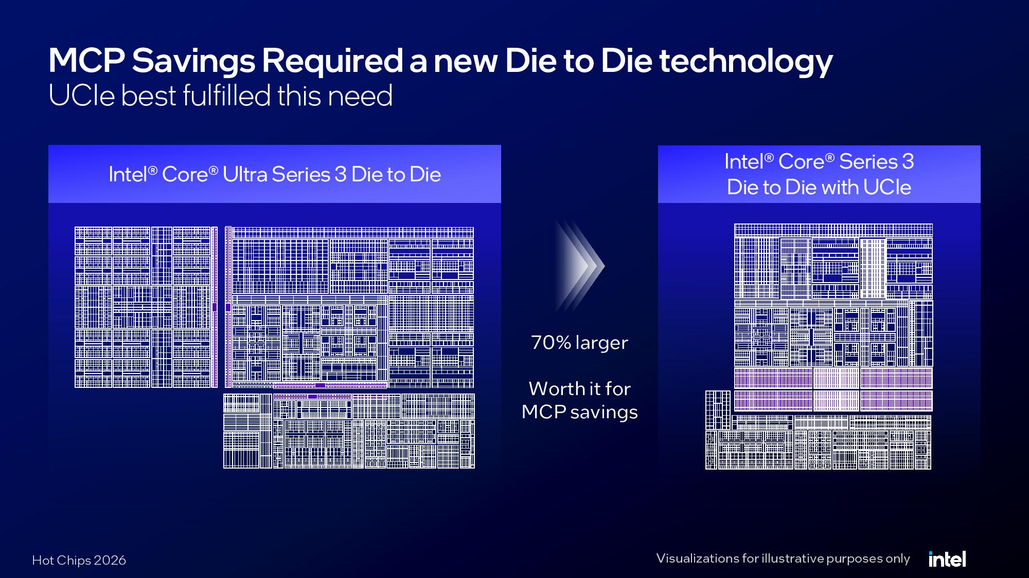
With 18A at the center of the compute and ISMC’s N6 handling the I/O die, Intel decided to make an MCP, which comes with some considerations. Advanced packaging allows designers to spend less die space on interconnects and use less power. With UCIe, Wildcat Lake’s interconnect is 70% larger than that on Panther Lake, and even then, Intel says the change was worth it from a cost perspective.
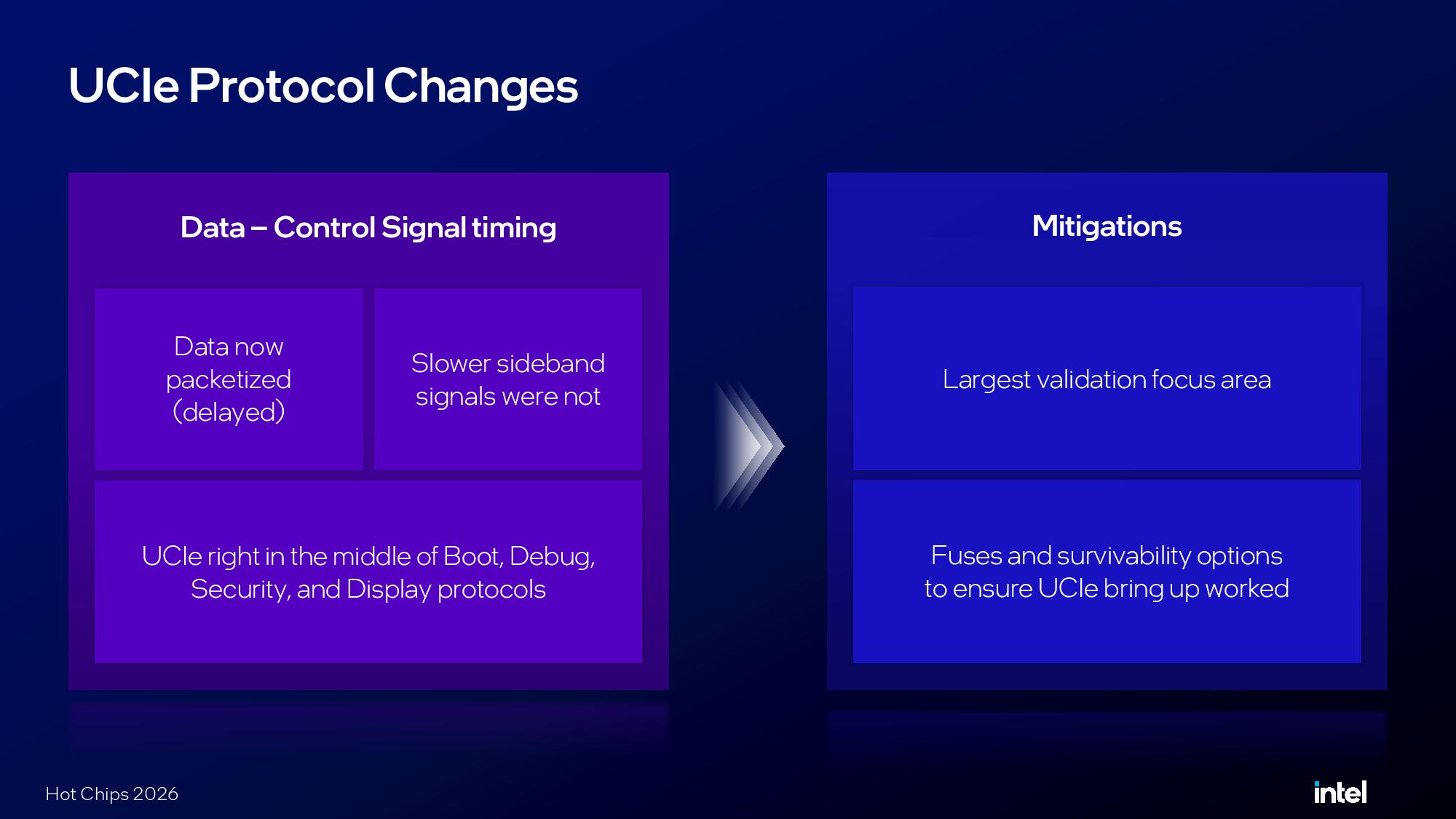
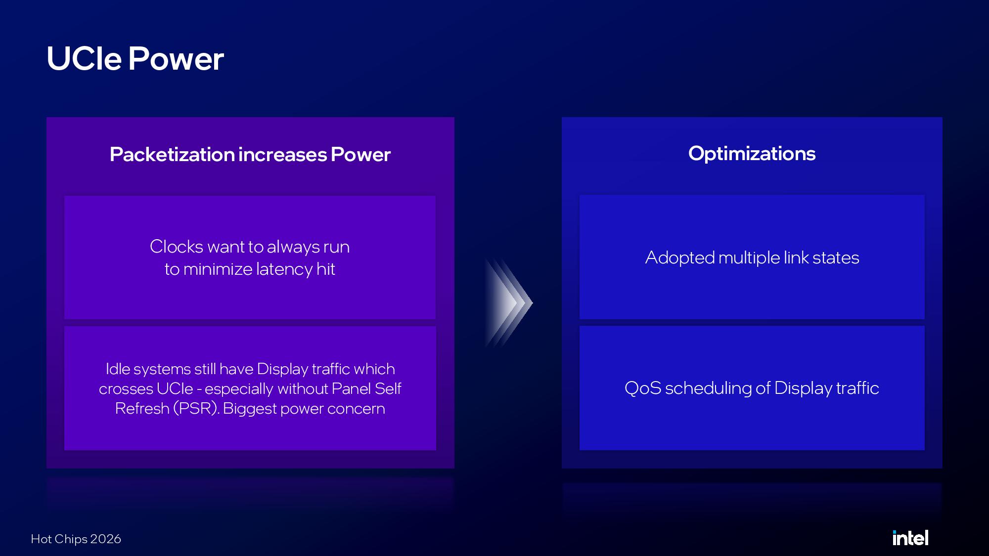
Outside of space, power was the primary concern with using UCIe. Battery life, especially for a budget part meant to handle lighter workloads, is extremely important, and UCIe brings increased power demands. UCIe die-to-die is packetized, which led to a challenging design point, particularly around the display.
Intel says that idle systems without panel self-refresh were the “biggest power concern,” as display signals need to cross the UCIe connection. To address the issue, Intel says it built a buffer to hold panel refreshes while the system was idle. This buffer is before the UCIe link, and it serves as an additional output buffer alongside the typical display buffer between the memory controller and display engine.
Without a base die for interconnect communication, UCIe also represents a large increase in die area. Intel trimmed a lot on both the compute and I/O dies to account for UCIe.
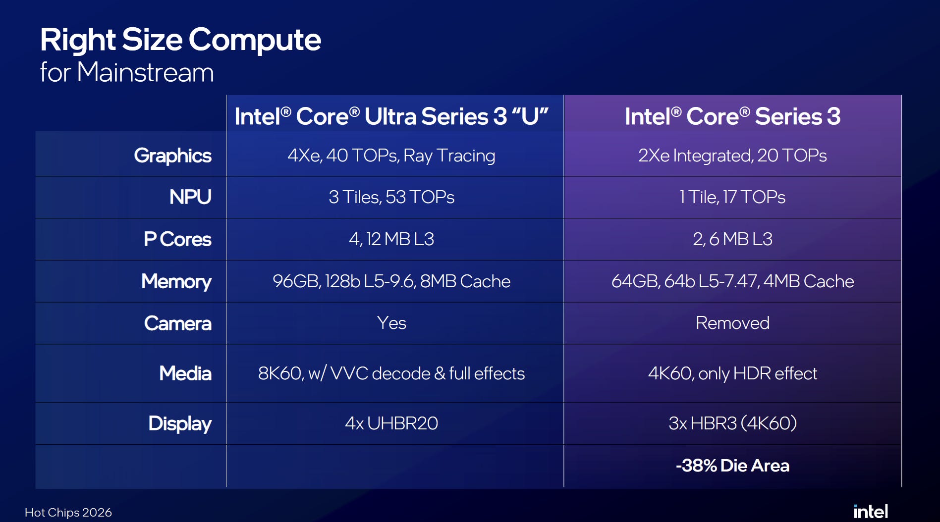
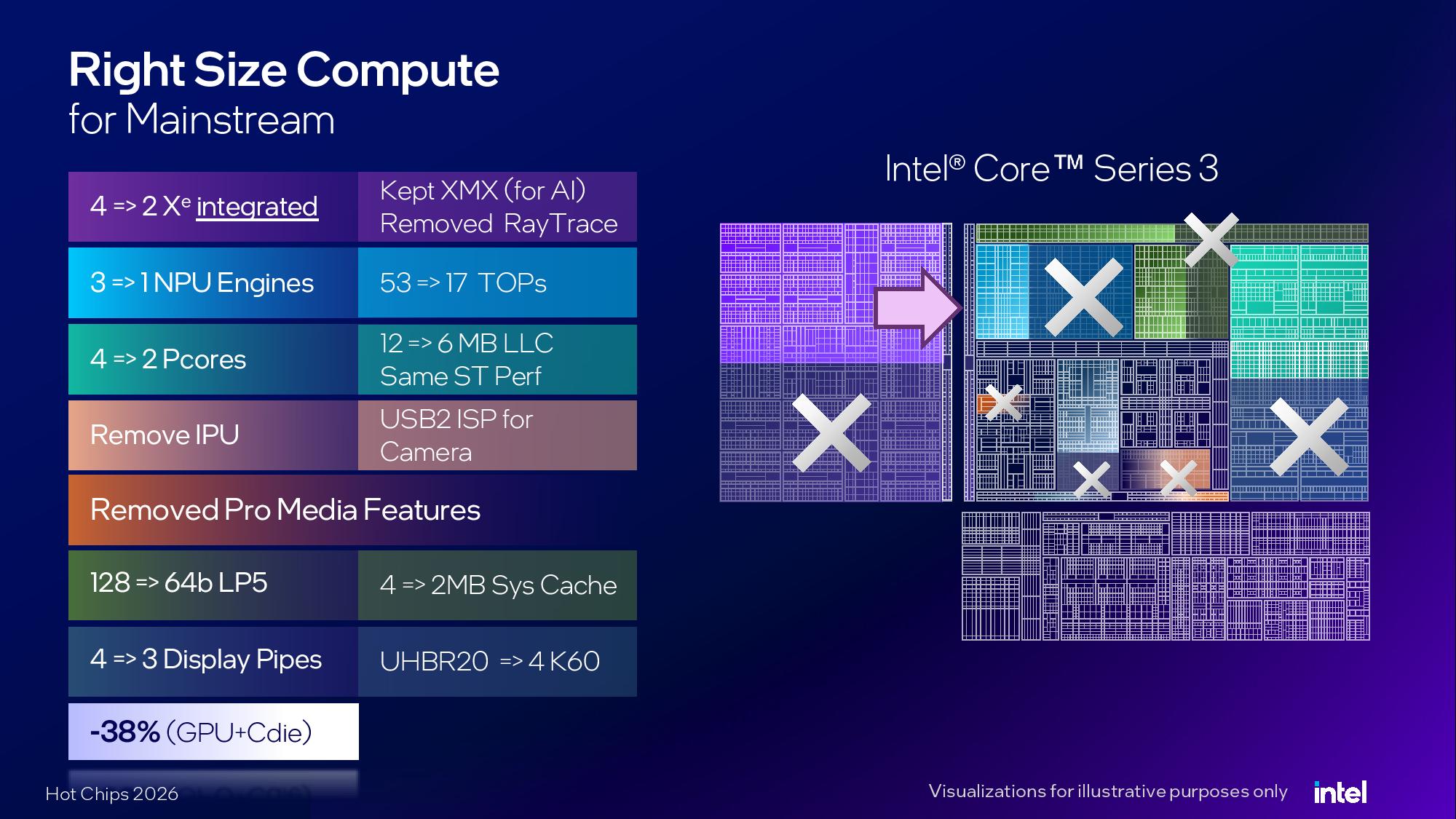
On the compute die, Intel trimmed down everything. Four Xe cores dropped to two, and without a dedicated ray tracing accelerator, the NPU went from three tiles to a single tile, and the memory subsystem was downgraded to a 64-bit bus, with lower maximum speeds and lower capacity. As mentioned, there were a lot of cuts in the display engine, which was a primary concern for die space and power.
Intel uses three display pipelines instead of four, opting for HBR3 as opposed to the massive bandwidth offered with UHBR20. That still provides 4K60 and can drive three external displays, which is plenty for a device in the class that Wildcat Lake is targeting. Trimming down the compute die allowed Intel to claw back 38% of its die space.
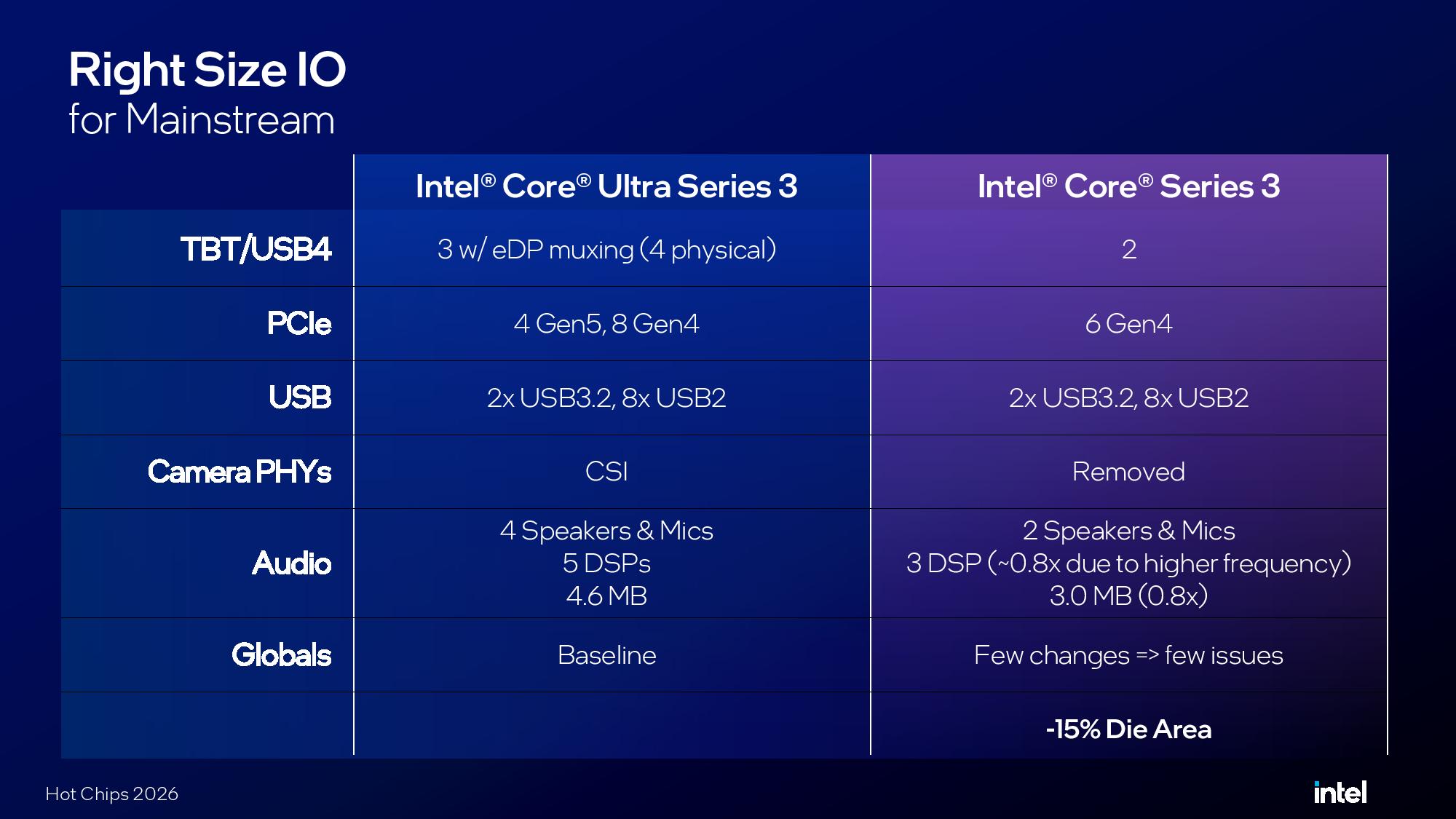
On the I/O die, Intel claimed back 15% die area by removing the camera PHY, reducing PCIe and USB support, and slimming down the audio engine. The camera was completely removed, placing the onus on OEMs to integrate their own controllers.
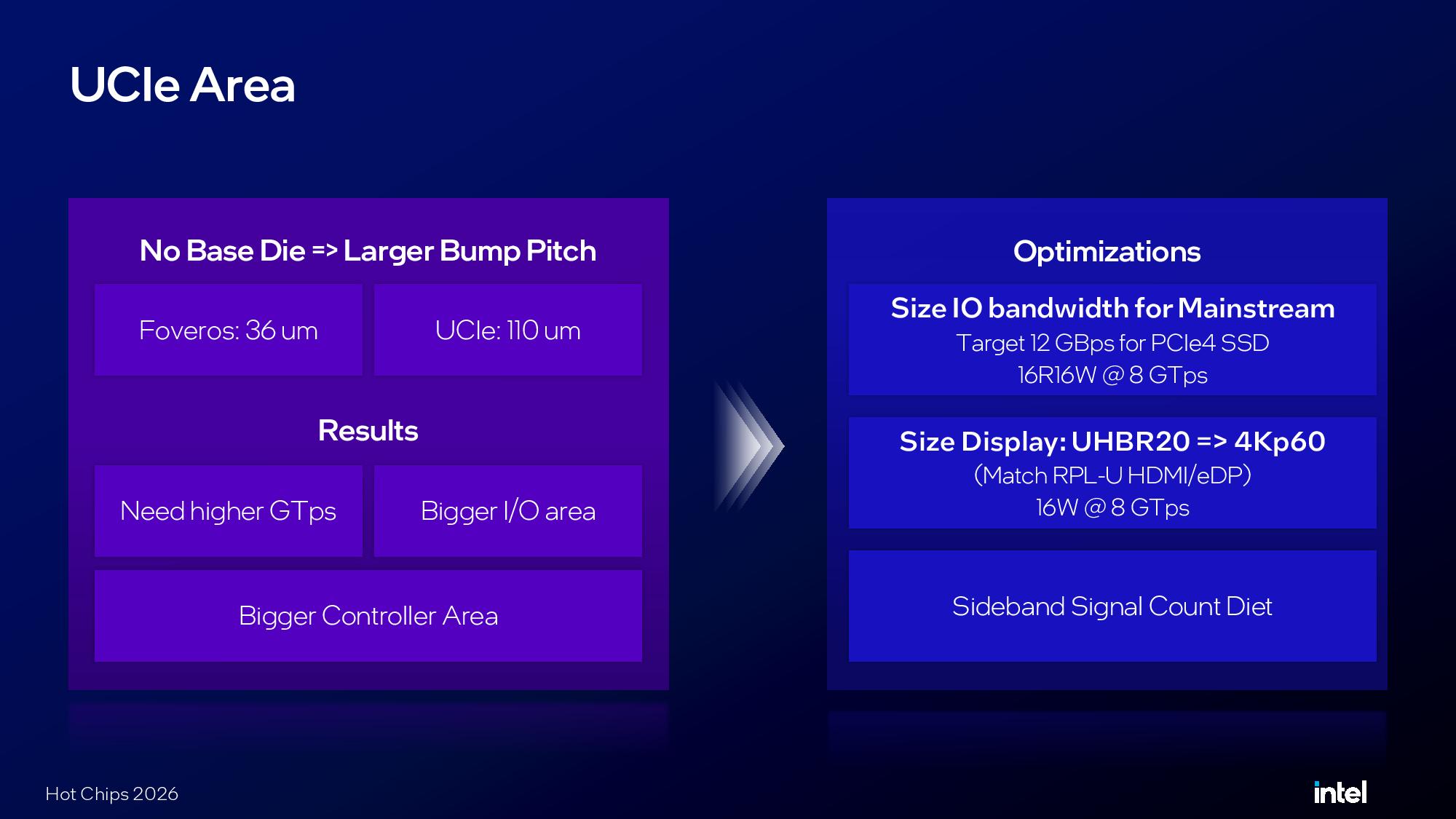
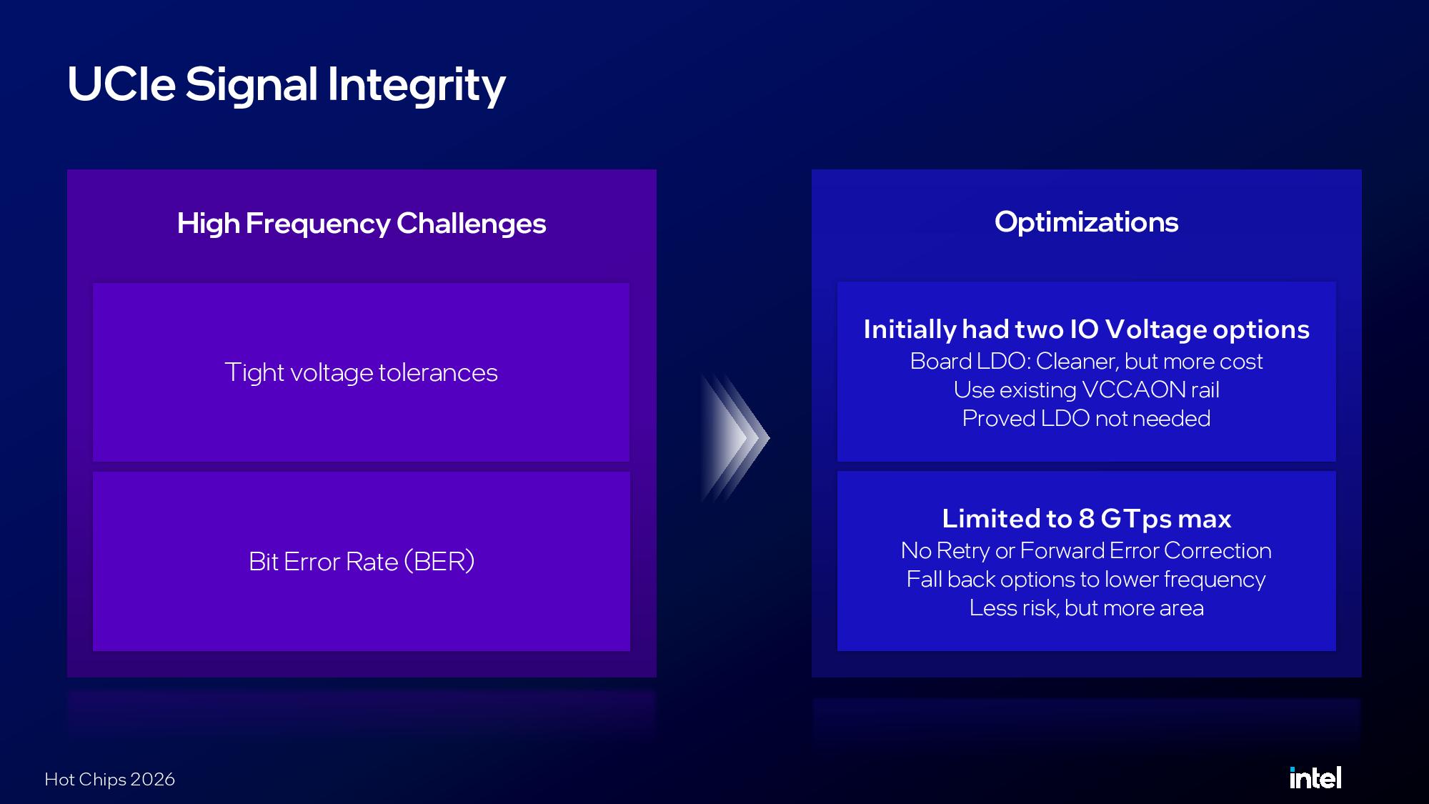
UCIe 3.0 is capable of up to a data rate of 64 GT/s, but Intel capped the transfer rate in Wildcat Lake at 8 GT/s. That still allowed Wildcat Lake to support mainstream PCIe 4 SSDs and 4K60 external displays, but running at a lower data rate reduces bit-rate errors and therefore allowed Intel to remove some bit-correction systems.
Reducing the cost of Wildcat Lake
Cutting down the compute and I/O dies saves money, but there are several other considerations when talking about the cost of a mobile SoC like Wildcat Lake. The economics need to work in the final product, which Intel touched on in its Hot Chips presentation, both from the perspective of the total bill of materials for OEMs and the yield/loss rate.
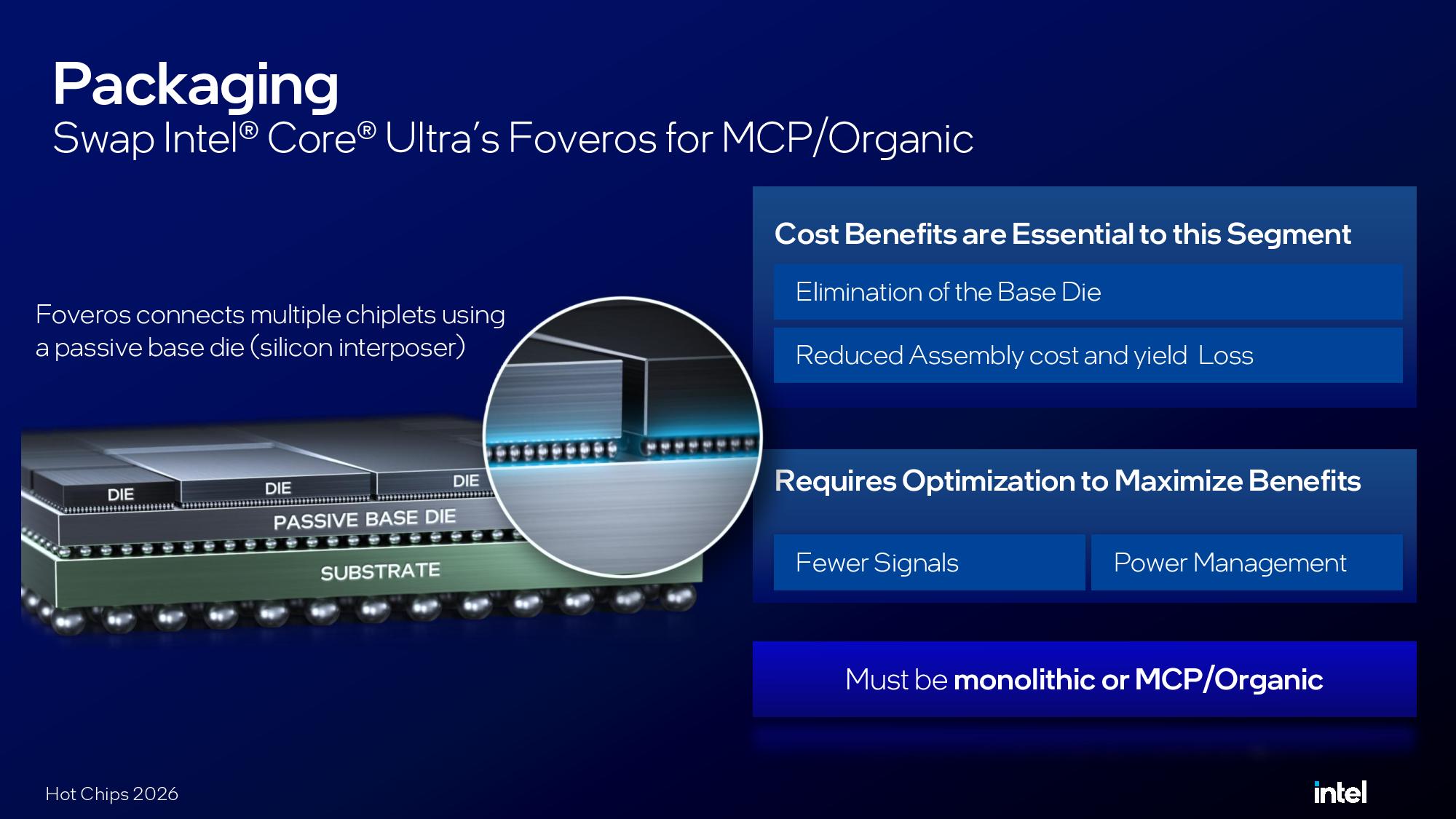
The big factor in cost savings was the elimination of the base die, which not only reduces raw material costs but also comes with the yield upside, without advanced packaging.
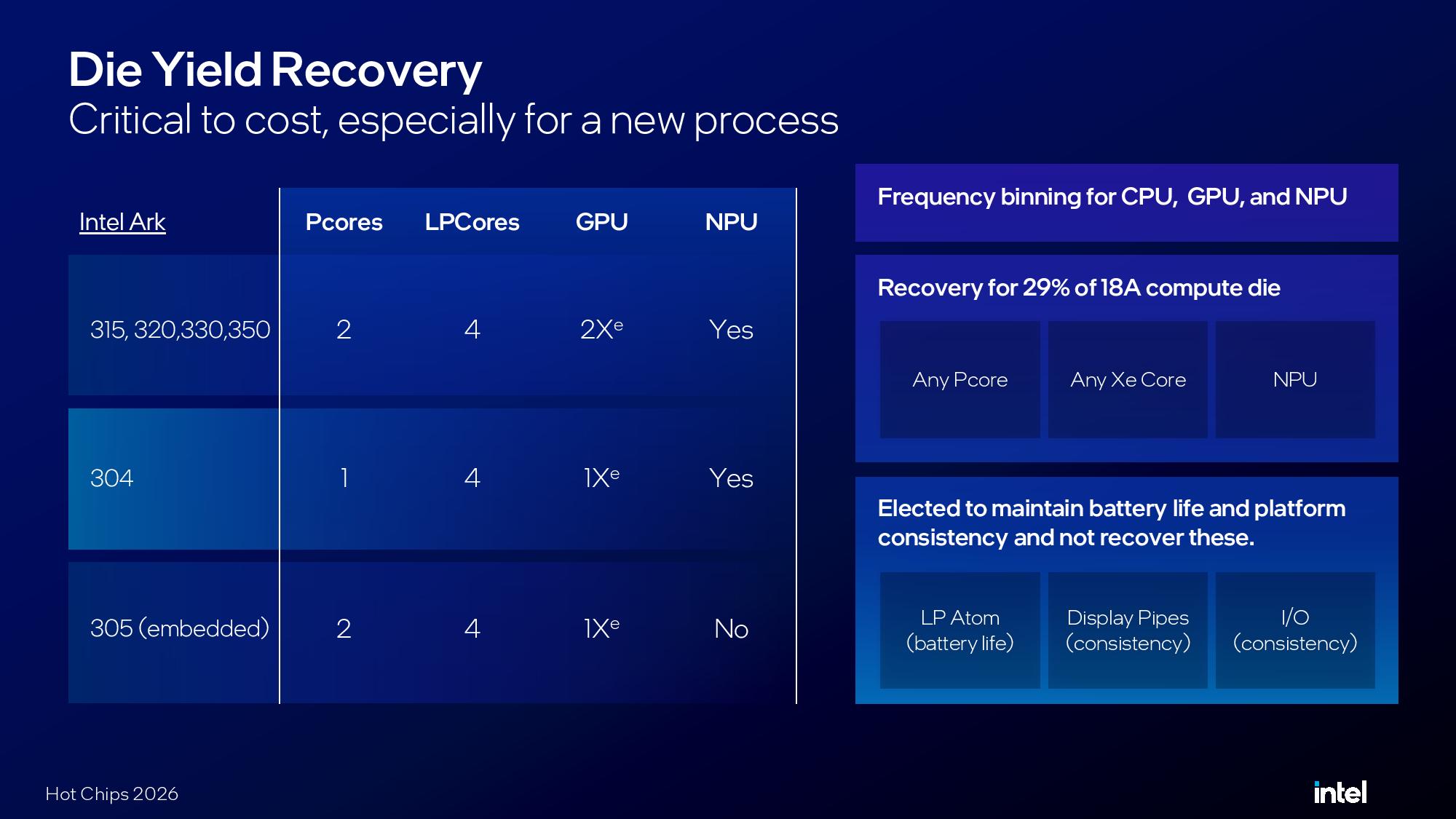
As usual, Intel bins Wildcat Lake into different SKUs, though it was careful to only attempt recovery where it could. For instance, it could package a single working P-core as a Core 3 304 instead of a 320. However, it didn’t attempt recovery in areas that would compromise key design points of Wildcat Lake.
For instance, it didn’t attempt recovery on LPE clusters and I/O, as they’re critical components of Wildcat Lake. The goal, according to Intel, was to create a stack that customers actually wanted to buy while trying to maximize yields where possible.
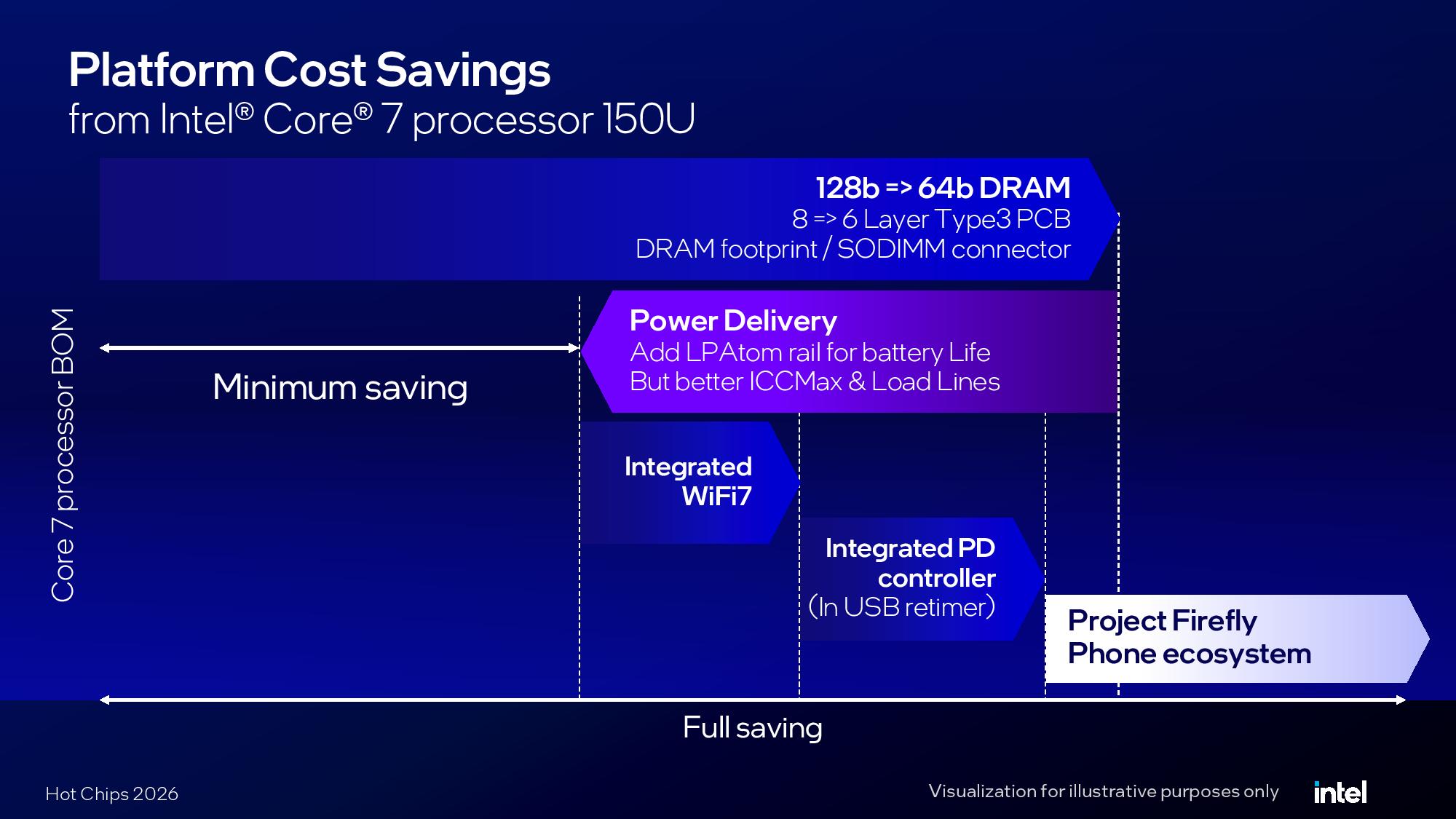
Intel also considered the full bill of materials for Wildcat Lake. Intel integrated Wi-Fi 7 and a USB PD controller, cutting costs for OEMs to integrate their own controllers. Perhaps the biggest point of savings was in memory, using a much slimmer bus and a 6-layer PCB as opposed to eight layers. Extending off the chart above is Project Firefly, Intel’s initiative to leverage the mobile supply chain for budget laptops.
Interestingly, Intel also included an area that led to higher cost but met the design goals of Wildcat Lake, that being a dedicated power rail for the LPE cluster. The “low-power island,” as Intel calls its LPE cluster, is critical to Wildcat Lake considering every SKU comes with only one or two P-cores. That dedicated power rail allows the vast majority of lightweight workloads to run on the LPE cluster and earn back battery life.
Wildcat Lake is one of the more interesting consumer launches we’ve seen in the past year. There’s the MacBook Neo and Snapdragon C competing in the same space, but both use mobile SoCs in the traditional N-1 design point for budget platforms. Wildcat Lake is different, based on Intel’s latest node, and leveraging newer open standards to achieve a lower price. That’s why it won a Tom’s Hardware innovation award for 2026, after all.
Full Intel Wildcat Lake Hot Chips 2026 presentation