Intel patent reveals new XBM memory architecture that ditches HBM’s costly silicon interposer — backend-transistor DRAM stack uses UCIe links and built-in repair to ease AI’s memory bottleneck
An Intel patent application published on July 2, 2026, surfaced by Underfox, has revealed the company’s plans for a new high-bandwidth memory (HBM) architecture that aims to ease the packaging and cost bottleneck of today’s interposer-based HBM. The patent application — filed back on December 26, 2024 — describes what Intel calls cross-batch memory (XBM), an “ultra-high-bandwidth memory with backend transistors” built with the goal of matching HBM4’s footprint while swapping conventional DRAM and its ultra-wide interface for back-end-of-line (BEOL) transistors and serial Universal Chiplet Interconnect Express (UCIe) links.
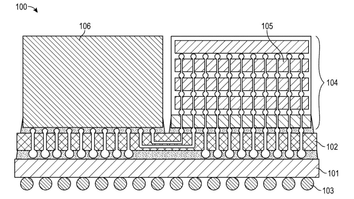
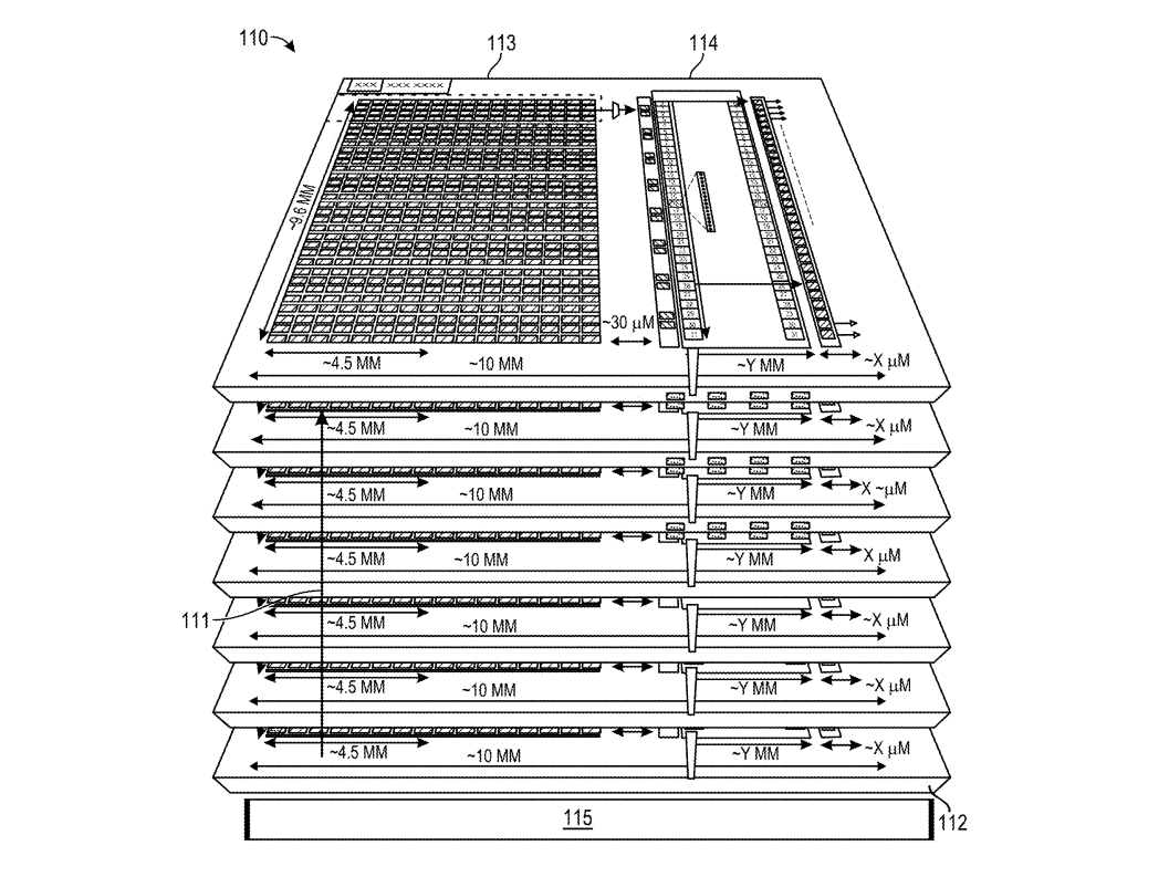
Intel’s proposed design is a memory stack that addresses the assembly costs that make conventional HBM expensive by dropping the costly silicon interposer and shrinking the package, while building in its own defect repair.
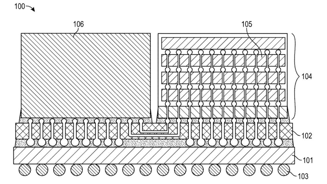
The filing lays out a stack of memory dies, each holding one-transistor one-capacitor (1T1C) DRAM fabricated in the back-end-of-line, wired together with through-silicon via (TSV) “gutters” and both-sided high-bandwidth interconnect (HBI) connections. Intel describes dies of roughly 1.5 gigabytes (GB) apiece — 768 “datablocks” arranged in a 32-by-24 grid, grouped into eight channels of eight sub-channels each — stacked eight high and scaling to 16. Data then leaves the stack over UCIe I/O bundles running at 32 gigatransfers per second (GT/s), funneled out through a base die.
To understand what Intel is changing, it helps to recall what standard high-bandwidth memory does. HBM stacks DRAM dies vertically on a base logic die, threads them together with TSVs, and communicates with the processor across a silicon interposer using an extremely wide parallel interface — on the order of 1,024 bits per stack. This width is how HBM delivers its bandwidth, but it is also what makes it expensive to package and hard to scale, as every one of those wires has to be routed through an interposer sitting between the memory and the compute die. As AI accelerators have outrun the rate at which memory can feed them, this “memory wall” has become the dominant constraint on performance, which is why nearly every large chipmaker is now attacking the interface and the stack rather than the logic.
XBM’s first major change is structural. Conventional DRAM cells are built in the front-end-of-line, the base silicon layer where transistors are normally fabricated. XBM instead moves the 1T1C cell into the back-end-of-line, the metal-and-via stack above the transistor layer, using thin-film transistors. Building memory in the BEOL is what lets Intel pack the die into many small, independently addressable memory blocks, and it is the same backend-transistor direction Intel has pursued for placing memory directly over logic.
The second change is the interface. Rather than HBM’s wide parallel PHY, XBM serializes data onto UCIe bundles at 32 GT/s, with the base die handling the serialize/deserialize step and routing all I/O to the compute die. Moving to a standard chiplet interconnect is what makes the design “chiplet-native” and, Intel argues, simpler and cheaper to package than an interposer-bound HBM stack. The tradeoff is that 32 GT/s is UCIe’s current top data rate, so the interface is already running at the spec ceiling rather than leaving obvious headroom.
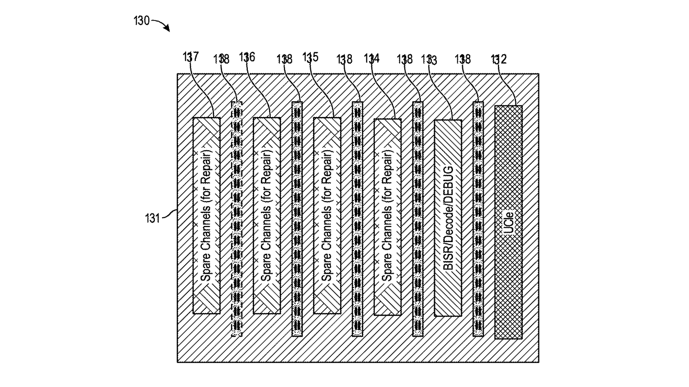
Intel also leans heavily on repairability. The base die carries dedicated spare channels, built-in self-repair (BISR), decode and debug logic, and four sub-channels of redundant memory arrays that act as fungible spares for defects in the dies above — post-assembly repair designed to claw back yield on a very tall stack.
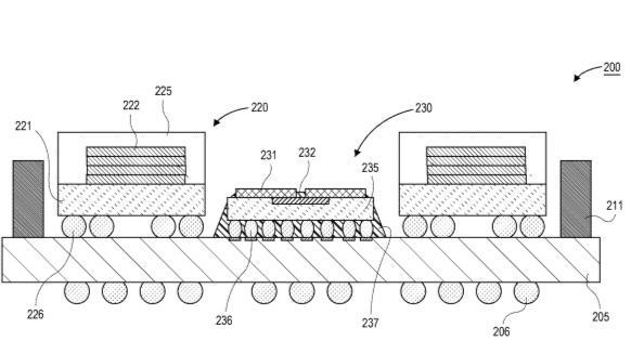
A large portion of the patent application focuses not on the memory cell at all but on how to mount it. Intel details memory-on-package (MoP) and “reversed overhang” structures aimed at cutting the stack’s Z-height — conventional MoP can add 300 to 350 micrometers (µm) — while removing the stiffener normally needed to control warpage and feeding DRAM power directly from the voltage regulator. This is the concrete basis for the “smaller, cheaper package” claim.
XBM should not be confused with ZAM (Z-Angle Memory), the architecture Intel is co-developing with SoftBank subsidiary SAIMEMORY and set to present at the VLSI Symposium 2026. ZAM’s innovation is on the bonding side — a fusion-bonded, nine-layer stack of largely conventional DRAM with roughly 3-µm-thin silicon between tiers — and it reportedly targets around twice HBM4’s bandwidth density, with commercialization aimed at 2029. XBM, by contrast, is an Intel-only filing that changes the DRAM transistor itself and the interface. Read together, they suggest Intel is running at least two parallel HBM alternatives, a fitting move for a company that began in 1968 as a memory maker.
The caveats on Intel’s proposed HBM architecture are the usual ones for a patent. The patent was filed 18 months ago, and there’s currently no product or roadmap, signaling potential intent rather than a shipping part. The UCIe interface is already at its rate ceiling, backend-transistor DRAM remains unproven at manufacturing scale, and the whole thing still has to justify itself against HBM4E and Intel’s own ZAM timeline.