New semiconductor firm breaks cover, backed by $43 million in early-stage funding — TYLsemi aims to deliver custom silicon to customers without breaking the bank
A new semiconductor firm, TYLsemi (pronounced Tile Semi), publicly revealed itself this month, alongside $43 million in early-stage funding and an ambitious plan to simplify the development of custom processors for AI infrastructure.
Dozens of contract chip designers can develop custom processors of different complexity. However, only a few companies can offer custom silicon design services using standard chiplets to speed up and derisk the development cycle. TYLsemi is aiming to join their ranks. We spoke to their founders to find out how the nascent business might pull it off.
Emerging from stealth
Rather than compete solely as another custom ASIC design house, TYLsemi intends to offer reusable, standards-based connectivity, power delivery, and eventually memory chiplets that customers can combine with their own differentiating compute silicon to build a unique system-in-package. For companies that do not intend to conduct semiconductor development themselves, TYLsemi will also provide an end-to-end service that includes design and implementation of a differentiating chiplet, packaging, qualification, and high-volume production, essentially enabling companies without any silicon development skills to offer their own multi-chiplet processors.
TYLsemi was co-founded by Mohit Gupta and Sunil Bhardwaj, semiconductor veterans who have led global engineering, operations, and business teams at Alphawave, SiFive, Cadence, Rambus, and other chip companies, and who collectively have plenty of experience with both standard and custom silicon. Mohit Gupta, a co-founder and chief executive of TYLsemi, believes that the time to establish a company that specializes in pre-approved chiplets and custom ASIC design is right now.
“Chiplets have been discussed for seven or eight years, but several things have changed in the last three or four years,” Gupta told Tom’s Hardware Premium. “First, advanced packaging has matured significantly. There are now multiple 2.5D and 3D integration options in volume production. Customers are not limited to one packaging technology or supplier; there are options from foundries and OSATs, including TSMC, Intel, ASE, and Amkor. Second, die-to-die standards have arrived. In the past, most chiplet implementations relied on proprietary interfaces. UCIe is now moving into production deployments, including at hyperscalers, which makes heterogeneous integration much more practical. Third, supply-chain resilience has become critical. Customers increasingly want modular and potentially multi-source strategies rather than a single point of failure. Those factors have created an environment that did not exist four or five years ago.”
AI accelerators will be among the primary applications to benefit from multi-chiplet design, as we have already learned from AMD and Nvidia.
“The AI accelerator market is on track to reach $604 billion by 2033, and custom silicon XPUs built for specific hyperscaler workloads are the fastest-growing segment,” Gupta said. “At that scale, chiplet-based design is no longer optional, yet there is no pure-play chiplet company serving this market with a full portfolio. TYLsemi closes that gap with standards-based chiplets combined with UCIe-based die-to-die connectivity, XPU-aware design, packaging, and integration — giving customers a fast, proven path to AI-era silicon.”
Chiplet economics
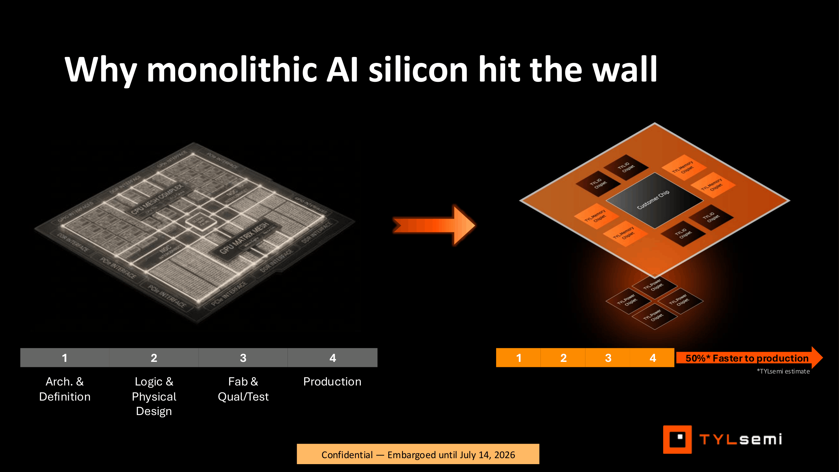
The vast majority of AI and HPC accelerators today feature large die sizes, in many cases approaching the size of a reticle. However, as modern process technologies are becoming more complex, foundries tend to increase their quotes for new nodes. A leading-edge wafer used to cost around $15,000 to process around five years ago, but today that price is around $30,000. As a result, large chips at a size close to the reticle limit implemented on a leading-edge node become an option for a select few chip designers who can afford it. For newcomers, multi-chiplet designs enabled by advanced packaging and standardized interconnects such as UCIe start to make a lot more sense.
“Once dies get into the 500 – 600 mm² range, the yield curve becomes increasingly difficult. Timing closure on a reticle-sized die is also challenging,” Gupta explained. “I have worked on a reticle-sized accelerator, and getting from 99% to the final 1% can require disproportionately more engineering effort.”
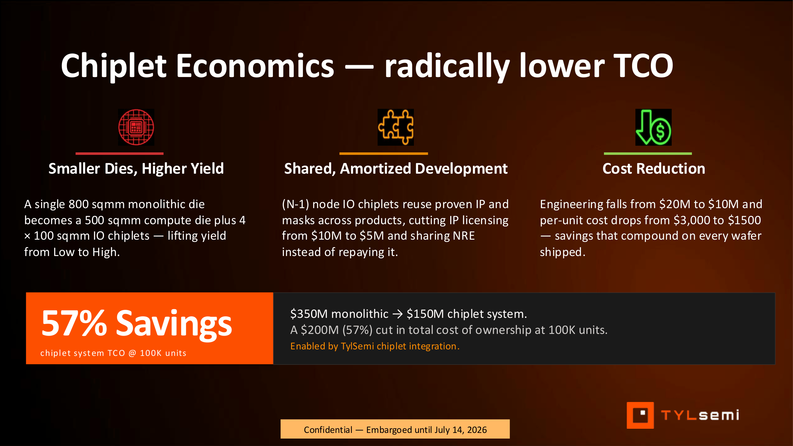
TYLsemi estimates that its chiplet approach could reduce total cost of ownership by 57% at a volume of 100,000 devices, from $350 million for a monolithic 700 mm² 3nm-class chip to $150 million for a design combining a 500 mm² 3nm-class compute die with four 100 mm² I/O chiplets built on an N-1 process. TYLsemi believes that the unit price of a monolithic chip would be $3,000, whereas the cost of an SiP would be around $600. The company attributes the saving to higher yields, reusable I/O silicon, lower IP licensing and engineering costs, and substantially lower per-unit silicon costs. However, the company stresses that the figures are illustrative estimates rather than actual manufacturing costs. Additionally, multi-chiplet designs can enable faster product refreshes compared to large monolithic dies as they are faster to develop and yield.
“Compute may move to 2nm or A14, while high-speed I/O can remain on 3nm, since I/O does not scale in the same way as logic,” Gupta said. “Our power-delivery chiplets can use an even less advanced process. Customers therefore do not have to use the most expensive silicon real estate for every function. […] There is no single answer for every design. You have to determine the right disaggregation points based on the architecture, thermal requirements, package, and how multiple accelerators communicate. […] The exact partitioning will vary by application, but you still get a better total cost of ownership.”
TYLsemi primarily targets AI infrastructure, so it generally envisions multi-chiplet designs to be used for AI accelerators, data-center CPUs, high-performance computing, networking and telecom silicon, and heterogeneous SoCs. However, TYLsemi has also ignored the fact that multi-chiplet designs are already widely used for consumer CPUs and GPUs.
Foundation chiplets
At the core of TYLsemi’s proposition are its foundation chiplets, which are reusable building blocks intended to handle common non-compute functions in custom AI and infrastructure processors and are implemented using various process technologies from TSMC. The foundation chiplets include the following:
- TYL.IO — a family of connectivity chiplets that includes TYL. IO PCIe, a 32-lane PCIe 7.0/CXL chiplet connected to the compute die via UCIe; TYL.IO Scale, a 224G+ SerDes for ESUN/UALink scale-up connectivity; and TYL.IO EIC for co-packaged optics.
- TYL.Power — a 16nm in-package IVR chiplet with embedded passives, designed to provide power closer to compute dies and use closed-loop control and die telemetry to improve power delivery.
- TYL.Mem — a planned family of memory-connectivity chiplets. TYLsemi has not yet disclosed the architecture or specifications, though it is safe to assume they are talking about memory controllers and PHYs.
Not all of these chiplets will be available immediately, as the company has certain priorities amid limited resources.
“The first TYL.IO product disaggregates the PCIe functionality that would normally sit on a large server processor, it is a 32-lane PCIe Gen7/CXL chiplet connected to the host compute die using UCIe,” Gupta explained. “The idea is that the CPU cores can move to 2nm, A14, or another leading-edge process, while the I/O chiplet remains on 3nm. The next product in the family will address scale-up connectivity between XPUs within a rack using high-speed SerDes. That device will be considerably larger, with around 72 lanes and approximately 14 TB/s of bandwidth. We also have an EIC roadmap for co-packaged optical connectivity. We expect samples of our first I/O product in the second half of 2027.”
These chiplets can be used as standalone components or integrated with a customer’s compute dies designed by the customer to TYLsemi through TYL.Forge, TYLsemi’s end-to-end custom silicon platform.
TYL.Forge
TYL.Forge is arguably one of the key enablers of TYLsemi’s business, as the program is aimed at companies that have their own compute architecture or even a compute die, but cannot build their own SiP or manage the entire semiconductor supply chain.
“There are larger custom silicon companies in the market, but many of them focus on a relatively small number of customers that can generate billions of dollars in annual business,” Gupta explained. “We see an opportunity among emerging AI companies and system companies that need advanced custom silicon but also need a partner capable of taking responsibility for the entire implementation and supply chain.”
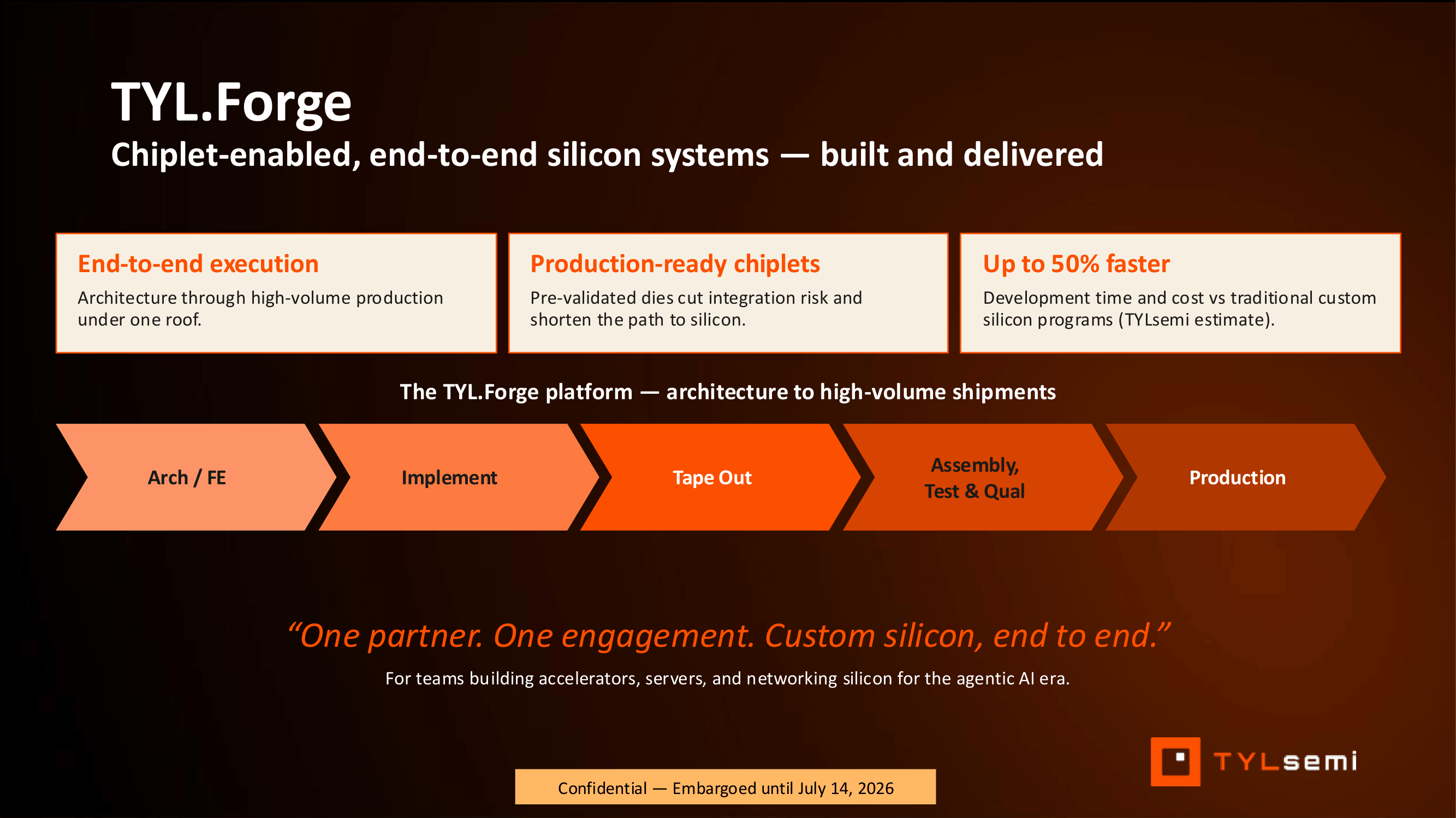
Such clients can provide their proprietary compute RTL, while TYLsemi handles physical implementation and integrates the resulting compute die with its pre-validated connectivity, power, and eventually memory chiplets. The company then manages tape-out, packaging, assembly, testing, qualification, and high-volume production.
“For example, a customer building a large accelerator can bring us its matrix-multiplication engine,” Gupta said. “We can implement the custom compute die and integrate it with our chiplets, so the customer does not have to reinvent the I/O and other common functions. This reduces risk and time to market.”
In fact, TYL.Forge appears flexible about where the customer enters the development process. TYLsemi describes the platform as covering everything from architecture and front-end design through implementation, tape-out, assembly, qualification, and production. So instead of RTL, customers can come to TYLsemi with an architecture/concept, and then the company will help develop and implement the silicon. Nonetheless, TYLsemi does not intend to invent the customer’s core compute architecture itself. In addition, customers can bring in an existing compute die, which TYLsemi can combine with its chiplets, package, test, and bring to production.
“We are also talking with companies developing Arm- and RISC-V-based server processors,” Gupta said. “They can develop the architecture, while we implement the rest of the silicon and bring the product to production. That gives customers an economic and engineering advantage because they do not need to build teams for every part of the chip.”
The key advantage of TYL.Forge is the reuse of pre-validated components. Instead of developing common functions such as PCIe connectivity and power delivery for every new processor, customers can use TYLsemi’s pre-validated foundation chiplets and focus engineering resources on differentiated compute architectures, software, and system design. In theory, TYLsemi could integrate third-party chiplets (not from a customer, but from a third-party chiplet provider). Still, the company’s focus remains on offering its own pre-validated chiplets and custom silicon with SiPs it builds.
“Potentially, [we could integrate third-party UCIe chiplets into a TYLsemi-based system], UCIe has done a very good job defining the electrical interface, but the ecosystem is still maturing at the protocol level,” Gupta explained. “In some cases, if we provide a chiplet to a customer, we may also need to provide or enable the UCIe IP on the other side of the connection. We are committed to UCIe and industry standards because standardization ultimately wins. […] We can consider customization for a large strategic customer or hyperscaler, but we do not want those projects to derail our standard product roadmap. […] Even when customers buy our standalone chiplets, I expect many of them will ask us to handle packaging and testing because heterogeneous integration and supply-chain management are difficult “
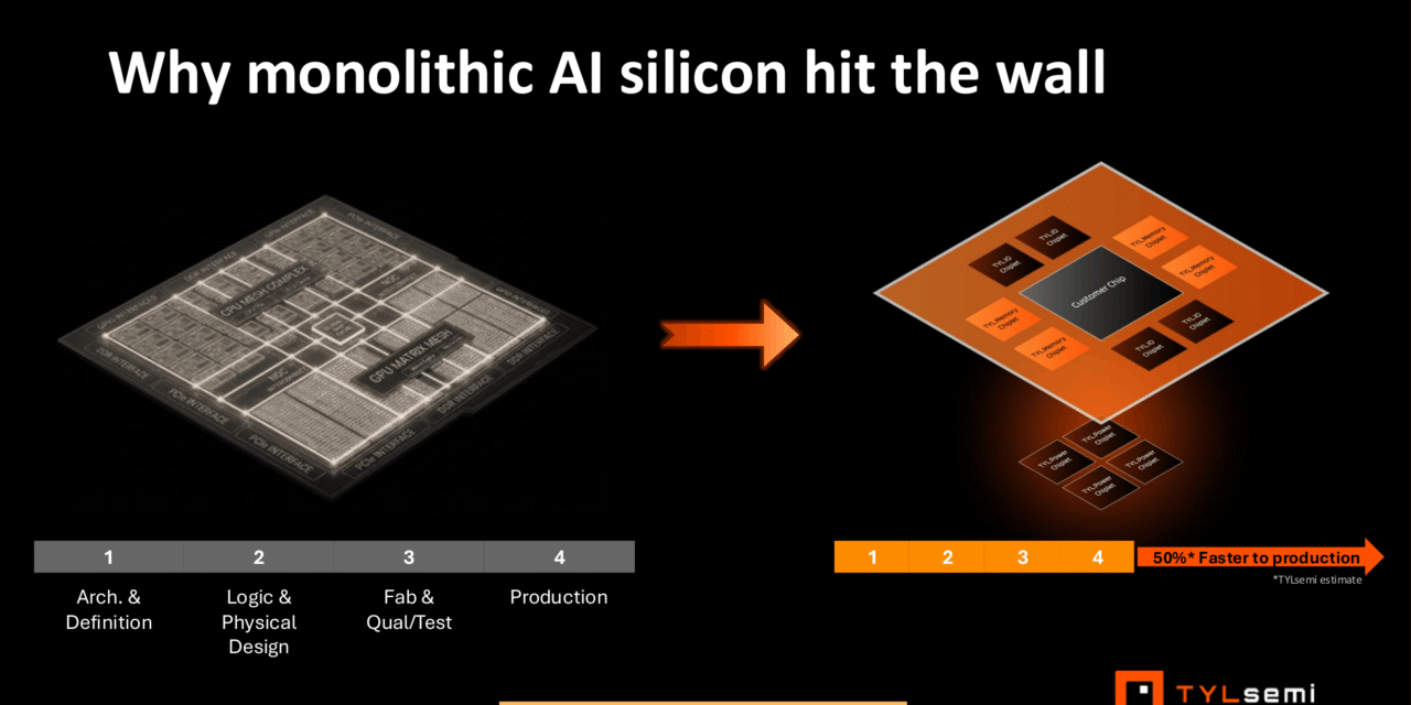
TYLsemi estimates that its approach can cut development time and cost by up to 50% compared with traditional custom silicon programs. In the best-case scenario, TYLsemi envisions that the development cycle can shrink considerably compared to today’s cycles that can be two, three, or more years long. According to TYLsemi, once a customer provides sufficiently mature RTL or a netlist, the company can take a custom compute die to tape-out in around six to nine months or so, which includes fabrication, assembly, testing, and qualification.
“If a customer provides mature final RTL or a netlist and uses our standardized I/O chiplet, we believe we can take the custom compute die to tape-out in approximately six months in some cases,” Gupta explained. “More generally, our target is six to nine months from a mature design to tape-out. The architecture and front-end phase is more customer-dependent. For a first-generation product, that can take around six months; for a more mature second- or third-generation design, it could be closer to three months, and some of that work can overlap with implementation. After tape-out, fabrication can take roughly four to five months depending on the process, followed by perhaps another two months for assembly, testing, and qualification. If the architecture is already mature, it may therefore be possible to reach production samples in about a year.”
Still, the company stresses that architecture development and implementation typically include feedback loops, which greatly slow the development process. This is why the company provides the relatively conservative ‘50%’ figure.
TYL.IO and TYL.Power samples will be available to qualified customers in 2027, in partnership with TSMC, and the company is looking forward to designing processors for its clients in time for them to reach the market in 2029 – 2030.
Speaking of TSMC, TYLsemi will initially only offer designs and services adhered to the TSMC ecosystem, though eventually it may offer other options for packaging technologies, such as Intel’s EMIB and Foveros, or Amkor’s packaging methods.
“We are initially focused on the TSMC ecosystem, but we also intend to explore other advanced-packaging supply chains,” Gupta said. “We do not want to limit ourselves to one packaging option. Over time, that could include other OSATs and packaging technologies. […] That could include Intel, ASE, Amkor, or others. Amkor, for example, is building significant packaging capacity in Arizona.”