
TSMC to start using High-NA EUV lithography in 2030 — A10 or A11 technology prime candidates for use
For years, TSMC has tried to avoid making public comments about its plans to use EUV lithography with a 0.55 numerical aperture optics, or High-NA EUV, because the company’s developers had a good idea how to keep advancing process technologies without using $400 million scanners. However, TSMC cannot rely on Low-NA EUV systems forever, so this week the company announced plans to use High-NA EUV starting from 2030.
- Analyzing TSMC’s fab expansion roadmap — multi-fab N2 ramp, CoWoS, SoIC, and uncorking bottlenecks
- Leading-edge foundry roadmaps for TSMC, Intel, and Samsung
- ASML’s roadmap for chipmaking lithography tools examined
- Chinese chipmaking tool roadmaps examined
TSMC did not formally reveal which fabrication technology will be the first to adopt High-NA EUV, though the year 2030 points to a few candidates. What TSMC did say is that it expects the number of layers processed using High-NA EUV to eventually increase as its fabrication technologies become more complex, driven by increasing complexity of transistor architectures, which is probably an implication for more sophisticated implementations of gate-all-around (GAA) transistors as well as complementary field-effect transistors (CFETs) later on.
TSMC plans to start using High-NA EUV lithography tools for high-volume manufacturing in 2030 using conventional 6×6-inch photomasks. The company then plans to build a pilot line that uses 6×12-inch photomasks in 2031 with the goal of bringing 6×12-inch High-NA lithography systems into advanced node production by 2033.
High-NA EUV lithography tools can achieve an 8nm single-exposure resolution, as opposed to a 13nm single-exposure resolution offered by today’s Low-NA EUV litho systems. However, when used with conventional 6×6-inch photomasks, High-NA EUV scanners have only half the exposure field of their Low-NA counterparts, which creates challenges for manufacturing very large dies. As a result, chipmakers building massive AI accelerators must either stitch multiple exposure fields together or adopt multi-chiplet designs, two approaches that have their own other challenges, such as tool productivity and power consumption. To circumvent the 6×6-inch photomask limitations, TSMC is working with ASML to set the stage for 6×12-inch photomasks.
Changing the size of photomasks is not a trivial endeavor as it requires changing everything from EDA software to tools that produce and write masks as well as systems that handle them, which essentially means that the entire industry must work on this change. ASML seems to be optimistic about the transition as it is supported not only by Intel and TSMC, but also by Samsung.
“We expect the adoption of High NA EUV to increase progressively along the device scaling roadmap, first using current 6-inch masks and then further supported by 12-inch masks, which enable greater scanner productivity and allow the industry to meet the demand for smaller, faster and more energy-efficient chips,” said Christophe Fouquet, president & CEO, ASML. “We are pleased by the strong initial support of semiconductor manufacturers, mask suppliers and partners for this initiative.”
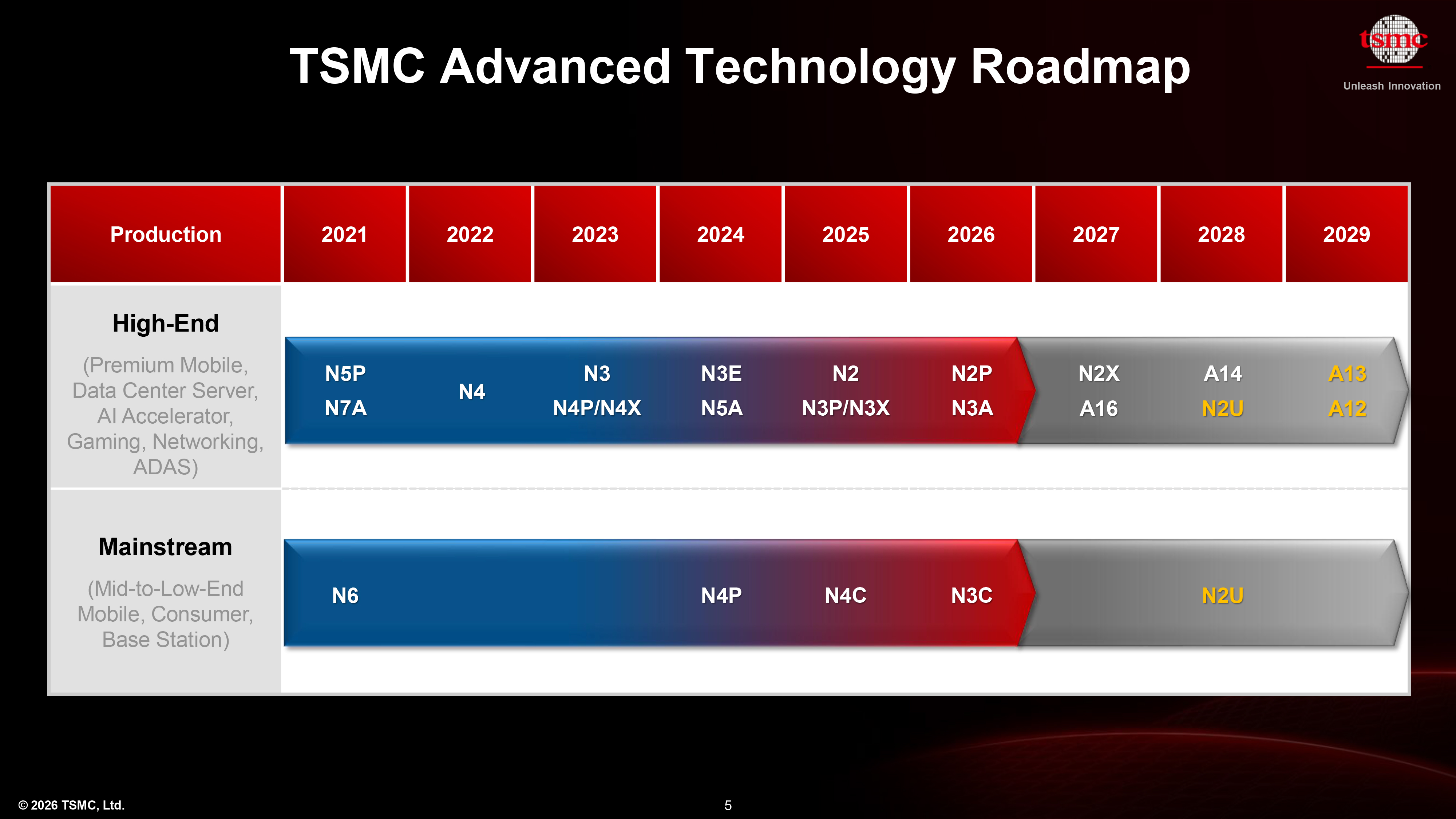
Perhaps the biggest intrigue about TSMC’s usage of High-NA EUV lithography is which process technology will be the first to use the new systems. Based on what we know about TSMC’s roadmap, A10 or A11 (1/1.1nm-class) seems to be by far the strongest candidates to use High-NA EUV scanners for the most critical layers. TSMC’s latest strategy separates its roadmap into annual client-oriented nodes (N2, N2P, N2X, A14, A13) and roughly biennial high-performance nodes (A16 in 2027, then A12 in 2029). The company has already confirmed that A12 and A13, due in 2029, will continue to rely on conventional EUV lithography.
Since A13 is an optical shrink of A14 that increases transistor density by only 6%, with performance and power improvements yet to be disclosed, its successor in 2030 will likely have to deliver considerably more substantial gains. It is therefore reasonable to expect A13’s successor — whether it is called A11 or A10 — to adopt more advanced lithography and/or TSMC’s 3rd Generation nanosheet GAA transistors to deliver significantly higher transistor density as well as meaningful performance and power improvements over its predecessor. Yet, we are of course speculating.